


What is "third-generation semiconductor"?
What is "third-generation semiconductor"?
The mainstream devices in power electronics are silicon-based MOSFETs, IGBTs, and thyristors, which have made outstanding contributions after more than 60 years of development. However, the performance of silicon-based devices has gradually approached their material theoretical limits, making it increasingly difficult and with limited room for improvement. Therefore, third-generation power semiconductor materials with superior performance have emerged.
Limitations of Si material properties:
·It is difficult to further reduce the conduction voltage drop (which determines the magnitude of on state loss)
·Low bandgap width (affecting high temperature performance)
·Low insulation breakdown electric field (affecting voltage resistance)
·Low saturation drift speed (affecting switch speed)
·Low thermal conductivity (affecting thermal design)
·
Characteristics of third-generation semiconductors:
Typical third-generation semiconductor materials:
·SiC (relatively mature, existing products)
·GaN (relatively mature, existing products)
·β - Ga2O3 (in development, with better performance than the above two types)
Comparing the three generations of semiconductor materials with Si parameters:
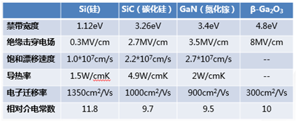
What do the above parameters represent? Taking SiC as an example:
·Forbidden width:
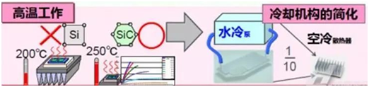
Third generation semiconductors have a higher bandgap compared to Si, which means higher chemical bond energy and stable high-temperature crystal structure. This is reflected in power electronic devices as high-temperature operational stability (simplified heat dissipation structure)
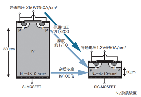
Insulation breakdown electric field:
Third generation semiconductors can withstand higher field strengths, thus achieving higher doping concentrations. For example, SiC epitaxial layers are thinner than Si at the same voltage level, resulting in lower on resistance of SiC power devices
a) Reduce thickness by 9/10 (same withstand voltage)
b) Increase doping concentration (proportional to square)
c) Devices with better performance (SBD instead of FRD, MOSFET instead of IGBT)
Saturation drift velocity:
Higher carrier saturation drift speed means higher switching speed. Due to the very low intrinsic carrier concentration and low leakage current of SiC, SiC devices have excellent reverse recovery characteristics
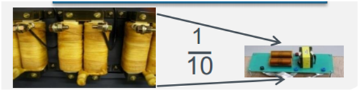
a) Faster switch speed
b) Miniaturization of peripheral components (inductors, capacitors)
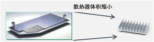
·Thermal conductivity: High thermal conductivity, easy to dissipate heat
a) Less thermal resistance
b) Miniaturization of heat sinks
c) Improve reliability and reduce the risk of device overheating failure (overheating is one of the main causes of power electronic device failure, accounting for about 70%)
The above characteristics can be summarized using radar charts:
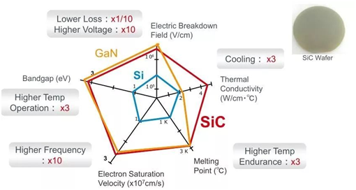
Image source: 2018 ROHM Exchange Conference
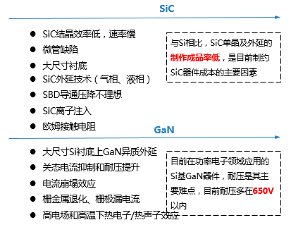
The difficulty of three and a half generations
Three and a half generations of application fields
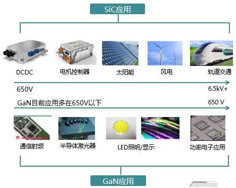
SiC tends to be applied in high-voltage, high-frequency, and high-power fields; GaN has more prospects in LED lighting, RF devices, LiDAR, and low voltage and high frequency fields
Taking new energy vehicles as an example, the application prospects of third-generation semiconductors are as follows:
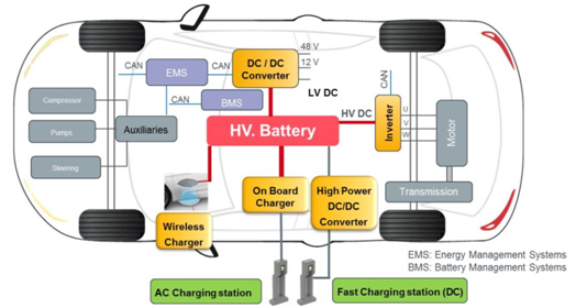
·In terms of new energy:
Motor controller
DC/DC
Car charger OBC
Wireless charging
DC fast charging
·Other aspects:
automative lighting
Laser radar
Taking the motor controller as an example to illustrate its advantages
Do you still remember when IGBT was born, why was MOS replaced by IGBT in the field of high voltage and high current
To withstand high voltage, Si MOS needs to be made thicker, which inevitably leads to an increase in the key parameter of on resistance Rds (on), resulting in significant losses;
Now SiC MOS can be made thinner, reducing Rds (on) and lowering conduction losses. At this time, the higher switching frequency of SiC MOS highlights lower switching losses, which is very advantageous in terms of efficiency for electric vehicle driving conditions
Simulation results:
The energy consumption of electric vehicles under WLTP cycles with different semiconductor technologies at 400V and 800V DC bus voltages reveals the potential energy consumption of SiC
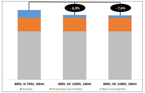
Source:
Effects of a SiC TMOSFET tractions inverters on the electric vehicledrivetrain PCIM Europe 2018
The main inverter of Tesla Model 3 using SiC MOS has been mass-produced
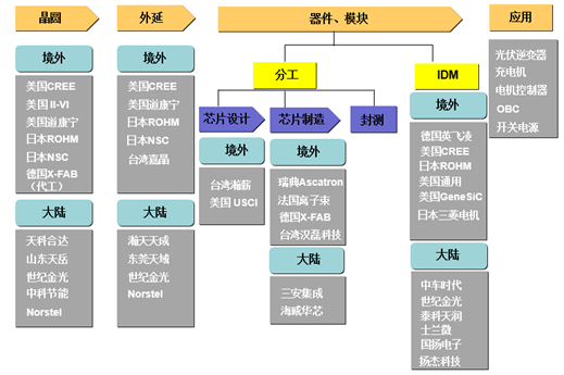
SiC Industry Chain Company
Summary
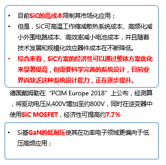
In the field of power electronics, the application of SiC can reduce volume and improve efficiency, which is currently recognized as a trend; As for the entire industry chain, it is currently limited by the production capacity of raw materials and chip manufacturing, and cannot be mass-produced on a large scale. However, according to Moore's Law of Hardware, the arrival of SiC may be faster than we imagine
Opportunities and challenges coexist, and we hope that the development of electric vehicles can quickly promote the development of the domestic IGBT and SiC industry chains
*Carrying Automotive Power Electronics
Talent Recruitment | Contact Us |

Copyright © 2024 Megateam Semiconductors(Shenzhen) Co., Ltd. All rights reserved